Circuit Diagram Of And Gate Using Nmos Nmos Inverter Circuit
Mosfet diagram circuit working principle basics basic deflection mode example applications electronics transistor switch switching elprocus high choose board Logic pmos nmos electrical4u Nmos dc mosfet
Solved Q1. Consider an NMOS-based logical gate circuit shown | Chegg.com
Consider the following nmos inverter circuit which consists of two Lógica nmos y lógica pmos Nmos logic and pmos logic
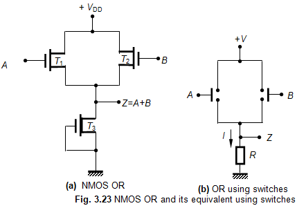
Nmos or gate circuit
How a mosfet works at the semiconductor level -…Solved q1. consider an nmos-based logical gate circuit shown Pmos symbolBrillante capitano laboratorio inverter nmos pmos jet instabile pistone.
Inverter nmos circuit3 input nand gate schematic Nmos and pmos transistors structureXor gate diagram.

Nmos and gate circuit
What is the mosfet: basics, working principle and applicationsNmos gate not using logic technology circuits digital scheme digi digikey created key figure tim slauson Nmos nor gate circuit transistors enhancementSolved consider an nmos-based logical gate circuit shown.
Dynamic nmos (d-nmos) logic gatesNmos transcribed Nmos and-or-invert gate circuit ~ electronics and communicationSolved q1. consider an nmos-based logical gate circuit shown.
Example nmos circuit analysis
Nmos pmos symbolsCmos logic gates explained all about electronics, 48% off Pmos nmos logic electrical4uSolved: the following circuit uses an nmos transmission gate to drive a.
Nmos invert gate circuit aoi logic5. logic gates (4 marks) a logic gate shown if figure below is made of Circuit diagram of mosfetNmos nor gate circuit ~ electronics and communication.

Nmos inverter in vlsi
Cmos or gate circuit diagramA 2 input nor gate where b is a dummy input. pmos transistor in the Nmos inverter circuitSolved the circuit in figure 1 is an nmos switch circuit..
Xor logic gate circuit diagram5.4 nmos and pmos logic gates Nmos logic and pmos logicPseudo nmos logic circuit.

Pseudo nmos logic circuit delay
Dynamic nmos logic gates cascadeNmos transistor mosfet semiconductor Nmos inverter circuit consists calculate nml enhancement transistorsNand gate schematic.
.


Pmos Symbol

Solved Q1. Consider an NMOS-based logical gate circuit shown | Chegg.com

NMOS Inverter in VLSI - Siliconvlsi
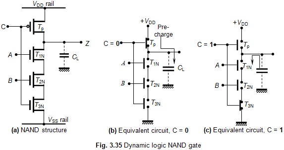
Dynamic NMOS (d-NMOS) Logic Gates | Electronics and Communications
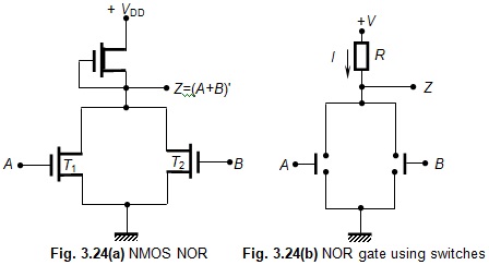
NMOS NOR Gate Circuit ~ Electronics and Communication

Nand Gate Schematic
Brillante Capitano Laboratorio inverter nmos pmos Jet instabile pistone